Exploring the Techniques of Nanotechnology Research
Written on
In the field of nanotechnology, researchers employ various sophisticated methods to examine their creations at the nanoscale. This article delves into how scientists and engineers utilize advanced microscopy techniques to investigate structures and devices that are only 1 to 100 nanometers in size.

The conventional optical microscope, often used in biology classes, has limitations. Although it can magnify samples up to 1000 times using visible light, its resolving power is restricted by physics, making it challenging to observe details smaller than 200 nanometers. This lack of resolution is insufficient for nanotechnology, where scientists work with atomic structures. Therefore, they rely on more advanced techniques to explore nanoscale features.
Electron Microscopy
Electron microscopy is a prevalent technique in nanotechnology labs, primarily categorized into scanning electron microscopy (SEM) and transmission electron microscopy (TEM).
In SEM, a focused electron beam is directed at the sample surface in a vacuum to prevent scattering by air. The interaction of the electrons with the sample produces a signal that is captured by a detector and converted into an image. SEM can achieve magnifications of approximately 1 million times.
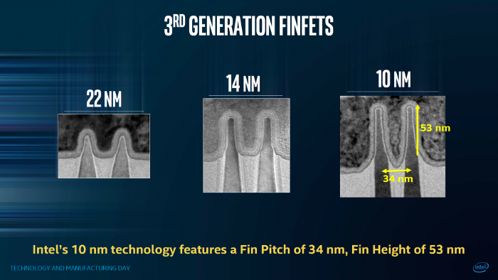
For even greater resolution, TEM is utilized, capable of magnifying samples over 50 million times. TEM images, such as those of Intel's latest transistors with 10 nm feature sizes, illustrate its power. In TEM, electrons are transmitted through thin samples, requiring meticulous preparation and significant voltage, leading to higher costs and complexity compared to SEM.
While SEM is the more frequently employed method due to its practicality, TEM is reserved for cases where higher resolution is essential.
Atomic Force Microscopy
When atomic-scale resolution of a sample's surface is required, atomic force microscopy (AFM) is the technique of choice. Here’s how it operates:
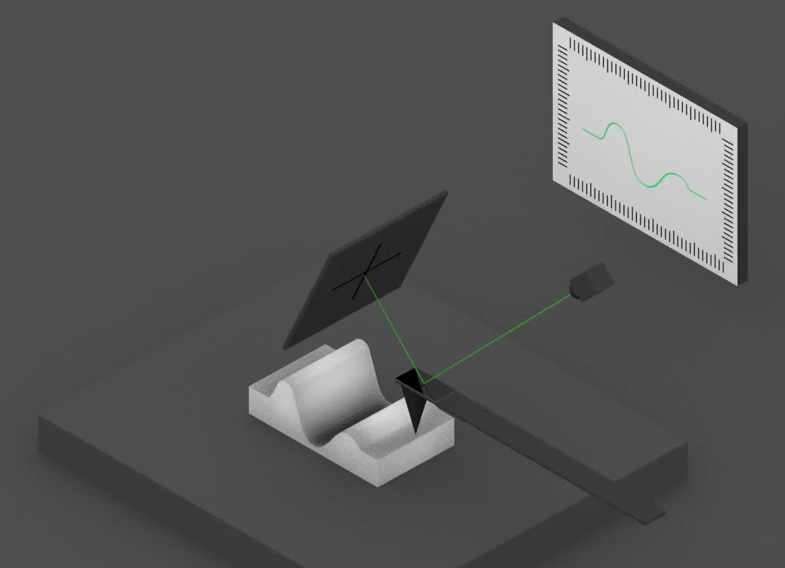
- A sharp tip, often smaller than a nanometer, is attached to a cantilever.
- A laser beam reflects off the cantilever, and any movement of the cantilever is detected.
- As the AFM tip scans the surface, it moves up and down according to the topography, allowing the computer to generate a detailed topographical image.
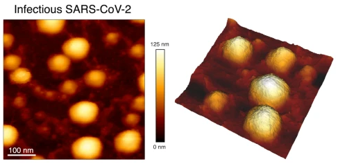
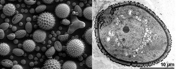
The image above depicts COVID-19 virions captured using AFM, highlighting the method's ability to reveal detailed surface structures.
Scanning Tunneling Microscopy
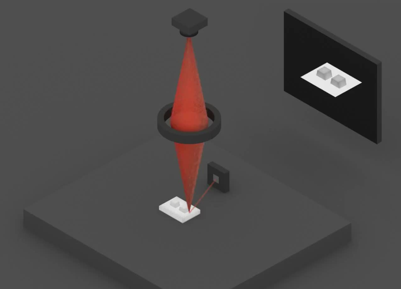
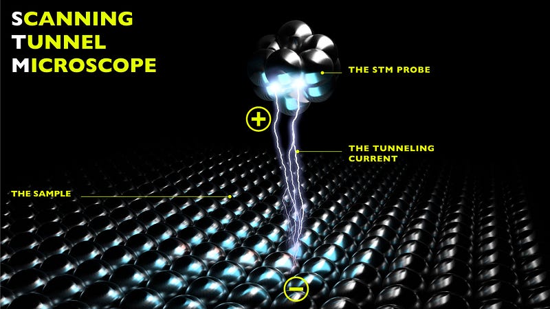
Lastly, scanning tunneling microscopy (STM) offers atomic-scale resolution and the capability to manipulate individual atoms. The process involves:
- Bringing an STM tip, which is about 1 atom wide, within 1 nanometer of the sample surface.
- Electrons can quantum tunnel through the minute gap to generate a measurable current.
- As the tip scans the surface, variations in current provide a topographical map of the sample.
STMs can also move individual atoms by leveraging van der Waals forces, allowing for precise manipulation.
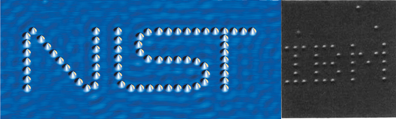
The ability to manipulate atoms has been demonstrated by spelling out names with individual atoms using STM technology.
In 1959, physicist Richard Feynman envisioned the potential of manipulating matter at the atomic level in his famous talk, "There's Plenty of Room at the Bottom." As tools for studying and creating materials at the nanoscale continue to advance, the possibilities for technological applications are boundless.
Thank you for reading! If you enjoyed this article, consider supporting my work by becoming a Medium member for unlimited access to articles.
If you liked this content, you might also find these articles interesting: 1. What Is Nanotechnology and Where Is the Field Today? — A historical overview of nanotechnology. 2. 3 Ways Scientists Can Unlock New Technologies by Working at the Nanoscale — Exploring the significance of nanoscale research. 3. Want to Make Contact with Aliens? Here’s How to Do It, According to Science — A review of scientific methods for potential extraterrestrial communication.
This article is based on a YouTube video I produced, which discusses the science and technology behind topics in science fiction. Check it out!
Citations: 1. Clay Dillow | Published Mar 23, et al. “Visible-Light Lens Can See Objects Tinier than the Light’s Wavelength.” Popular Science, 26 Apr. 2021, https://www.popsci.com/technology/article/2011-03/first-lens-image-sub-100-nanometer-resolutions-visible-light/. 2. “Electron Microscopy: Tem vs Sem: Thermo Fisher Scientific — US.” Electron Microscopy | TEM vs SEM | Thermo Fisher Scientific — US, https://www.thermofisher.com/us/en/home/materials-science/learning-center/applications/sem-tem-difference. 3. Atteberry, Jonathan. “How Scanning Electron Microscopes Work.” HowStuffWorks Science, HowStuffWorks, 12 Jan. 2021, https://science.howstuffworks.com/scanning-electron-microscope2.htm. 4. “Atomic Force Microscopy.” Nanoscience Instruments, 18 Feb. 2022, https://www.nanoscience.com/techniques/atomic-force-microscopy/. 5. “Scanning Tunneling Microscopy.” Nanoscience Instruments, 26 July 2018, https://www.nanoscience.com/techniques/scanning-tunneling-microscopy/. 6. Eigler, D. M., and E. K. Schweizer. “Positioning Single Atoms with a Scanning Tunnelling Microscope.” Nature, vol. 344, no. 6266, 1990, pp. 524–526., https://doi.org/10.1038/344524a0. 7. “Quantum Physics; Nanoscale Assembly; NIST Atom Logo.” NIST, https://www.nist.gov/image/quantumphysicsnanoscaleassemblynistatomlogojpg.